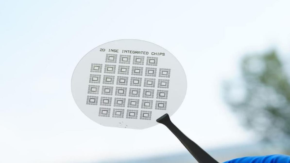
 Researchers at Peking University have broken new ground in semiconductor development. Using an innovative solid-liquid-solid process, they’ve produced the world’s first wafer-scale, two-dimensional indium selenide (InSe) chip. This 2-inch wafer boasts exceptional crystal quality and phase purity—qualities that not only challenge silicon’s long-held position but also offer a fresh avenue for next-generation chip manufacturing.
Transistors built from these wafers deliver electron mobility up to 287 cm²/V·s and precise switching performance at sub-10nm gate lengths, comfortably meeting the 2037 benchmarks of the International Roadmap for Devices and Systems (IRDS). This advancement easily dovetails with current CMOS processes, making it an appealing option for ultra-low-power AI accelerators, edge computing, and flexible electronics. If you’ve ever faced the struggle of overcoming performance limits in your projects, this breakthrough might just offer the inspiration you need.