 Hey there! If you’re interested in the latest advancements in electronics, you’ll want to hear about this. Researchers have developed an innovative technique that could change how we integrate two-dimensional (2D) semiconductor materials with dielectrics. This breakthrough might just pave the way for creating smaller, more efficient electronic devices.
For a long time, the challenge has been transferring these delicate semiconductors onto substrates without introducing defects. But this new method, which promises cleaner transfers and better device performance, could be the game-changer we’ve been waiting for.
The team behind this innovation comes from Peking University and the Beijing Graphene Institute. They’ve come up with a process that involves the epitaxial growth of ultra-thin dielectric films on graphene-coated copper surfaces. Published in Nature Electronics, this technique allows for the film to be transferred with fewer defects, which is a big deal in the world of microelectronics.
According to the authors Zhongfan Liu, Li Lin, and Yanfeng Zhang, the idea came from grappling with the persistent issues of integrating 2D materials like graphene into devices. Traditional methods often lead to contamination and stress, which can really mess with device performance.
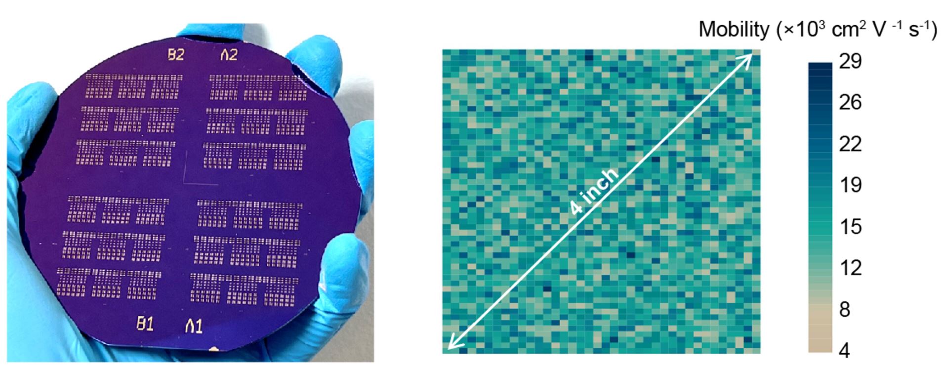
The process starts by synthesizing a single-crystal dielectric, antimony oxide (Sb2O3), on graphene that’s grown on a Cu(111) substrate. Li Lin explained, “We initially grow the Sb2O3 film on the graphene using a vacuum thermal evaporation process.” This approach has successfully transferred a 4-inch graphene wafer while preserving its electrical properties.
Looking ahead, this technology could help develop advanced electronics that combine 2D semiconductors with dielectrics. Lin mentioned, “We’ve managed to transfer a 4-inch graphene wafer intact, maintaining its intrinsic electrical properties while integrating it with single-crystal dielectric Sb2O3.”
As for the future, the research team is excited about expanding this approach to enable three-dimensional integration of 2D materials. They’re aiming to tackle challenges like interlayer coupling and interface control. Lin added, “We want to develop advanced transfer techniques that allow for stacking and precise alignment of 2D materials, creating multi-layer, three-dimensional integrated structures.” This could lead to high-performance, densely integrated electronic devices that are more powerful and efficient.


