 Imagine a world where AI hardware is not only faster but also far more energy-efficient. Thanks to a new platform developed by researchers using photonic integrated circuits (PICs) on silicon chips, that world is just around the corner. Led by Dr. Bassem Tossoun at Hewlett Packard Labs, this innovation is set to shake up the AI industry by tackling the big energy and processing hurdles that today’s AI systems face.
You might already know that modern AI systems, which lean heavily on graphical processing units (GPUs), are notorious for gobbling up energy and demanding tons of processing power. But here’s the exciting part: this new platform, recently detailed in the IEEE Journal of Selected Topics in Quantum Electronics, could dramatically boost both scalability and energy efficiency. Unlike the usual GPU-based setups, PICs use III-V compound semiconductors to run AI tasks with optical neural networks (ONNs). These networks work at the speed of light and lose very little energy in the process.
Dr. Tossoun explains the challenges and the promise of silicon photonics: “While silicon photonics are easy to manufacture, scaling them for complex integrated circuits is tough. Our device platform can serve as the building blocks for photonic accelerators that are much more energy-efficient and scalable than what we have now.”
The team has taken an innovative approach by mixing silicon photonics with III-V semiconductors, boosting the platform’s density and complexity. This combo allows for PICs that can handle all neural network operations, making them perfect candidates for the next wave of AI accelerator hardware.
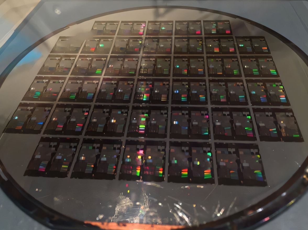
Here’s how it starts: fabrication kicks off with silicon-on-insulator (SOI) wafers, followed by processes like lithography and dry etching. The integration of III-V semiconductors such as InP or GaAs onto the silicon platform is done via die-to-wafer bonding. A thin gate oxide layer and a thick dielectric layer add to the efficiency and stability.
Dr. Tossoun emphasizes the platform’s significance: “The heterogeneous III/V-on-SOI platform provides all the essential components needed to develop photonic and optoelectronic computing architectures for AI/ML acceleration. This is especially important for analog ML photonic accelerators, which use continuous analog values for data representation.”
Thanks to this unique photonic platform, we can now integrate all the devices needed for building an optical neural network on a single chip. This includes active devices like on-chip lasers, amplifiers, high-speed photodetectors, energy-efficient modulators, and nonvolatile phase shifters. The result? A huge leap in energy efficiency, offering a footprint-energy efficiency that’s 2.9 × 10² times greater than other photonic platforms and 1.4 × 10² times greater than advanced digital electronics.
This breakthrough is set to cut energy costs and boost computational efficiency, opening the door for better AI-driven applications across many sectors. It promises to tackle computational and energy challenges, paving the way for a robust and sustainable future for AI accelerator hardware.