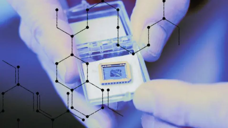
 Researchers from the National University of Singapore and the University of Manchester have developed two smart approaches that boost graphene’s electronic performance beyond traditional semiconductors. It’s impressive to see graphene’s electron mobility now surpass gallium arsenide (GaAs), a material honed over many years.
Graphene—a single-atom-thick layer of carbon atoms arranged in a honeycomb lattice—is celebrated for its strength, flexibility, and exceptional conductivity. Still, if you’ve ever worked with cutting-edge electronics, you know that no material is without challenges. In graphene, performance dips at cryogenic temperatures due to electronic disorders from nearby charged defects, which cause electron-hole puddles and scatter electrons.
In one approach, Assistant Professor Alexey Berdyugin’s team used extra graphene layers as an electrostatic shield against environmental disturbances. By twisting two layers at a significant angle, they achieved electronic decoupling, considerably reducing charge inhomogeneity and allowing quantum behaviours to emerge at lower magnetic fields.
The second method, led by Nobel Laureate Sir Andre Geim and Dr Daniil Domaretskiy, explored a proximity metallic screening technique. By positioning graphene near a metallic graphite gate—separated only by an ultrathin dielectric barrier—their setup drastically minimised disorder, setting record Hall mobilities.
These strategies expand the available toolkit for developing advanced two-dimensional materials, potentially accelerating progress in high-speed electronics and quantum technologies. For anyone keen on electronic innovation, the methods show how creative tweaks can pave the way to exploring pristine electronic behaviours.


