 Researchers at Pohang University of Science and Technology have developed a fresh approach to fabricating high‑performance tin‑halide perovskite thin‑film transistors (TFTs). By switching from traditional solution‑based methods to an innovative vapor deposition process, they’ve addressed long‑standing production challenges and paved the way for more reliable, scalable electronics.
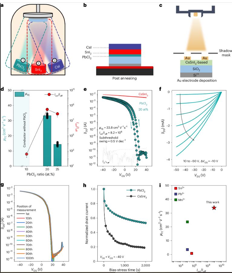
Tin‑halide perovskites boast a unique crystalline structure reminiscent of calcium titanate, offering an appealing alternative to conventional semiconductors. If you’ve ever wrestled with creating uniform, high‑quality films on a large scale, you’ll appreciate how this new method overcomes those hurdles. The study, recently published in Nature Electronics, explains how a sequential deposition of lead chloride (PbCl2), tin iodide (SnI2), and cesium iodide (CsI) transforms precursor materials into excellent cesium‑tin‑iodide (CsSnI3) films.
Professor Yong‑Young Noh, who leads the research, explains that the PbCl2 layer doesn’t just sit there—it kick‑starts the solid‑state reaction that turns the mixture into a robust perovskite film. This clever maneuver not only ensures uniformity but also enhances the hole density in the transistor channels, a critical factor for performance. The resulting p‑channel transistors deliver average hole mobilities of 33.8 cm²/Vs and boast on/off current ratios around 10⁸, clearly surpassing earlier solution‑processed devices.
The advantages extend beyond the lab. With OLED production already using similar thermal evaporation methods on large substrates, this vapor deposition technique fits naturally into existing manufacturing frameworks. Moreover, it opens up exciting opportunities for vertical stacking of perovskite layers, offering a route to more advanced circuit designs without relying on conventional, solvent‑based photolithography.
Looking ahead, Professor Noh and his team are committed to further refining the process. They’re exploring fresh compositional variations and advanced materials engineering approaches, aiming to lower processing temperatures and reduce production costs. This focus on continual improvement could well make tin‑halide TFTs a staple in future semiconductor applications.


