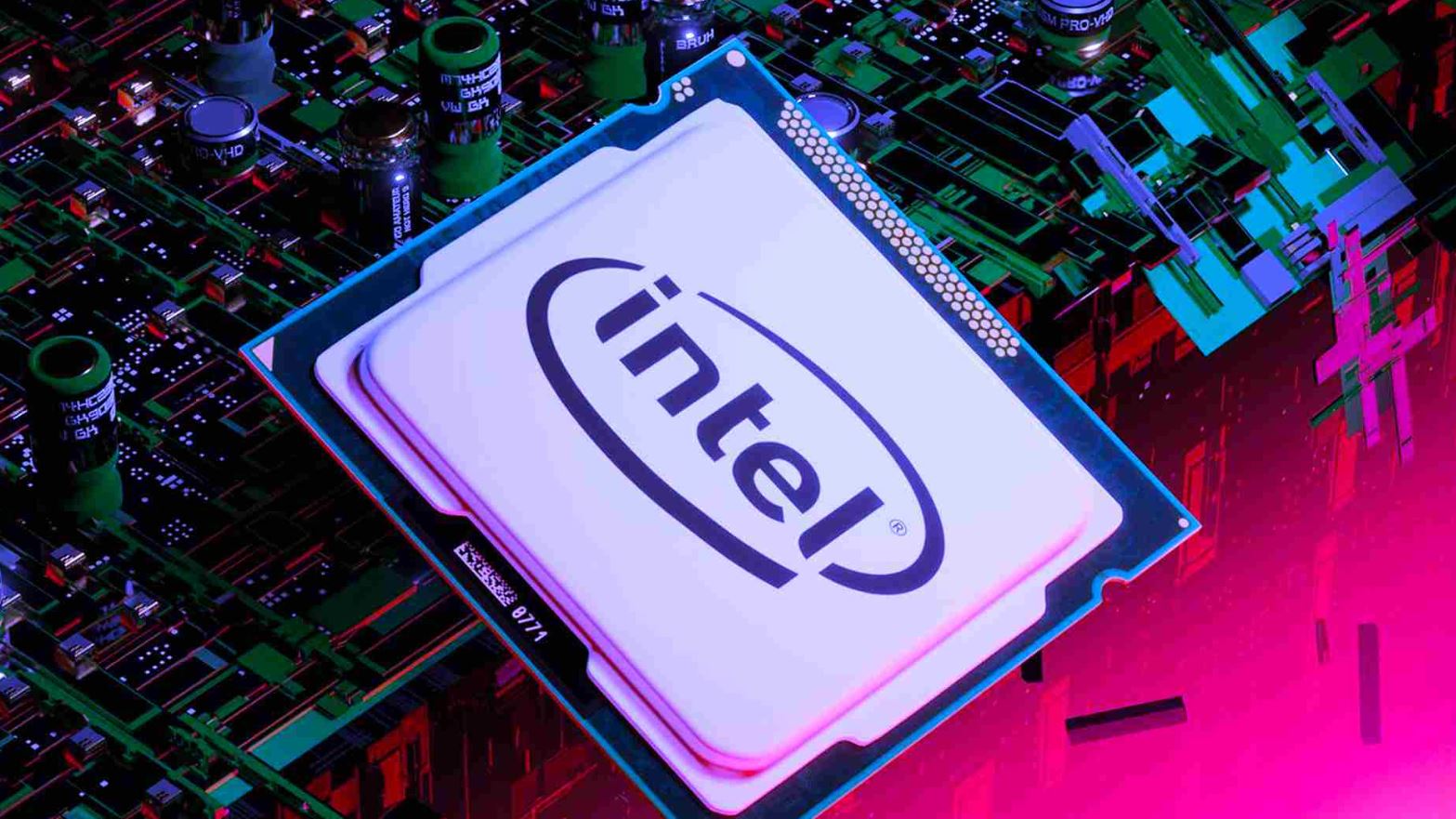
 At the recent IEEE Electronic Components and Packaging Technology Conference, Intel introduced a host of refined chip packaging technologies designed to boost AI processing. As Moore’s Law faces mounting challenges, combining multiple silicon dies into one seamless package promises to meet the growing demands of AI.
Because a single chip is limited to around 800 square millimetres, these innovations let manufacturers pack in more than 10,000 square millimetres of silicon into a package that spans over 21,000 square millimetres – roughly the combined size of four credit cards.
A key element in this new approach is the Enhanced Multi-die Interconnect Bridge (EMIB), now upgraded to EMIB-T. This version features through-silicon vias (TSVs) – tiny vertical channels that directly connect power pathways – which helps minimise energy loss, while a copper grid cuts down on electrical noise for steadier performance.
Intel has also refined its low-thermal-gradient thermal compression bonding technique. By improving how silicon dies attach to substrates, this method manages differences in thermal expansion between materials, paving the way for larger and more reliable chip assemblies.
Another important development is the segmented heat spreader, designed for efficient thermal management. Its modular design dissipates heat effectively, ensuring stable performance even as temperatures rise.
While these developments are still in the research phase, Intel expects them to hit the market within a few years. If you’ve ever struggled with the limitations of current chip designs, this fresh approach could be the breakthrough you’ve been waiting for.


